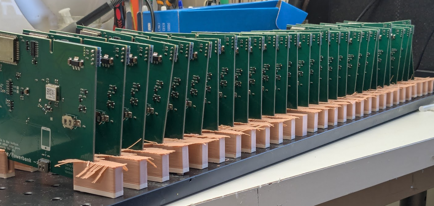
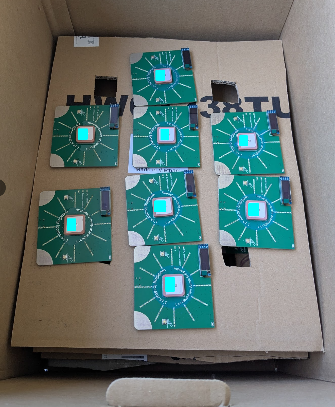
The boards have arrived:
It’s covered in lead
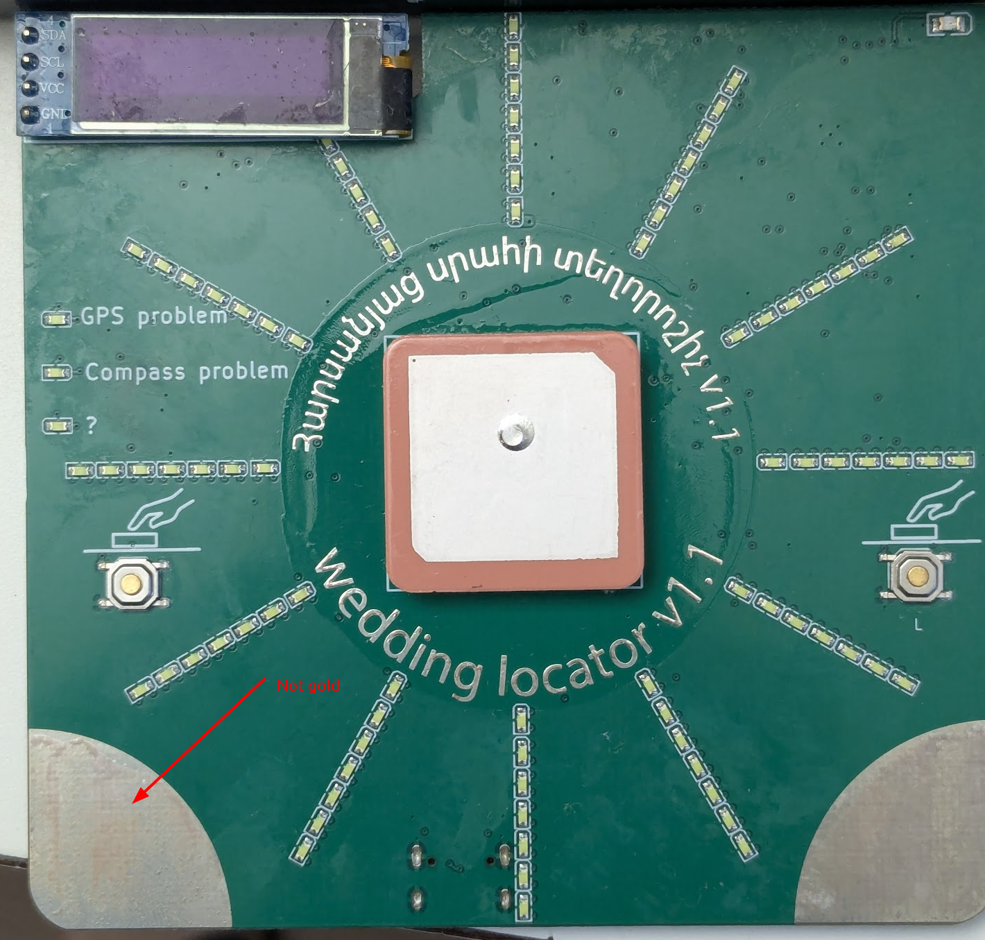
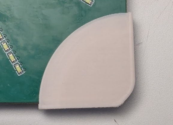
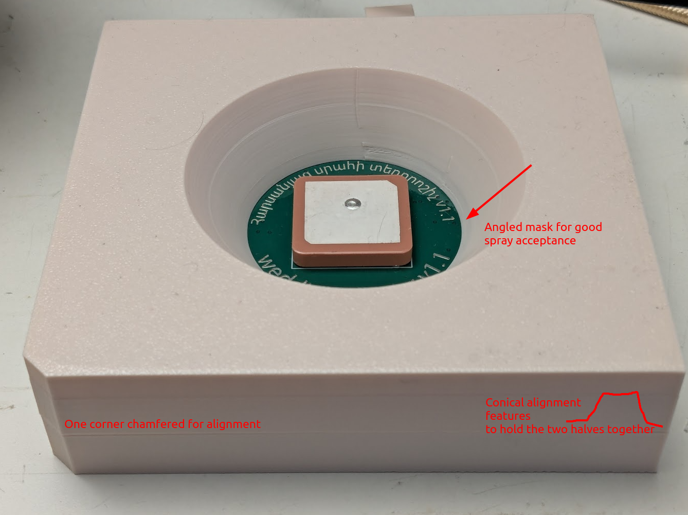
The default surface finish option when ordering from JLCPCB is HASL with lead. I did so many dry runs through the ordering process that I forgot to pick ENIG. Now all the lovely pads that people are supposed to hold onto are coated with lead. I aim to address this by conformal coating the text, and 3D printing coverslips to go over the finger pads:
Since I don’t trust the conformal coating not to scratch off under constant rubbing.
Actual functionality
Seems fine as far as I can tell. Have not programmed all the PCB’s yet, but the few that I have operate fine. I got claude to add a self check program to see that data was coming in from the imu, compass and gps as well as that a valid i2c transaction could be issued to the screen. All boards have worked so far.
Personalised names
I’ve laser etched the name of each of the attendees on all the PCB’s. Here is a zoomed in photo of one of the letters:
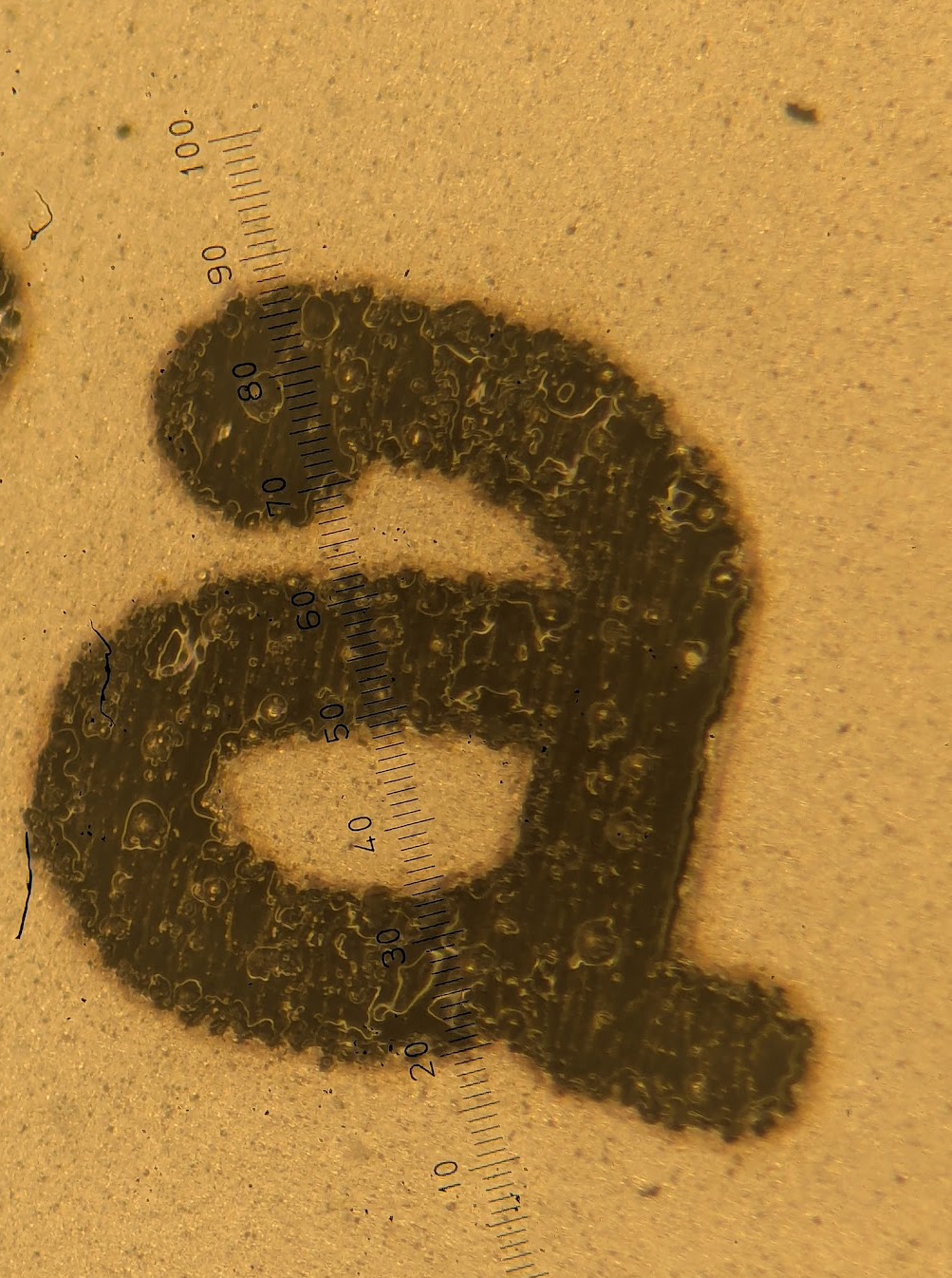
Pretty good!
Conformal coating application
Here is the mask I used to only apply the coating to the writing:
I thought about selectively masking out the switches, USB port, screen, and battery holder selectively so that the whole board could be coated but it seemed like less effort to just selectively coat the center text instead.
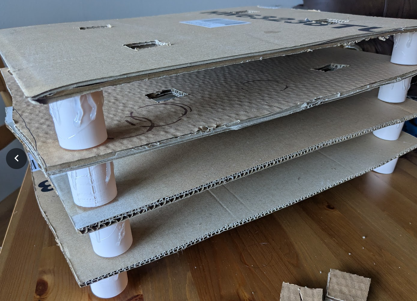
The conformal coating needs to be cured for a while so to get it done faster I built a small hair dryer powered incubator in which all the PCB’s could be stacked at once and held for 50C for a few hours to cure them:
Here are the stacked racks, which together with the floor of the cardboard box was just able to accomodate the 40 PCB’s.
Here is the box in operation:
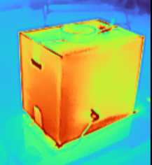
Nice and toasty.
Importance of esp32 antenna PCB cutout
The layout guidelines for the esp32 module said that there should be a cutout in the PCB around the antenna, so the first revision of the board included this:
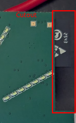
Since the first revision of the board did not use any wifi features, and the cutout was kind of annoying, and I figured surely it wouldn’t be that important anyway, I removed it for the second revision of the board and didn’t even bother to pull the ground plane away:
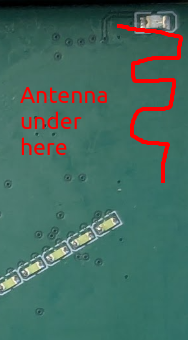
However I just added a cool new feature to the PCB whereby all the boards would continuously broadcast and listen for each other. Then when another was found, they would use the compass feature to point to each other so you could find another wedding attendee in e.g. the airport, which would be cool.
However the signal drops out after moving only ~10m or so away, so I asked mr claude to write a simple script that measured the rssi between two of the PCB’s, and I made this measurement with the two of the new revision PCB’s, and then one old and one new:
  ┌──────────────────┬────────────────────────────┬────────────────────────────┐
  │                  │ A sees B (B's TX → A's RX) │ B sees A (A's TX → B's RX) │
  ├──────────────────┼────────────────────────────┼────────────────────────────┤
  │ Old B (AE:E0:04) │ -66 dBm                    │ -67 dBm                    │
  ├──────────────────┼────────────────────────────┼────────────────────────────┤
  │ New B (B0:64:E0) │ -43 dBm                    │ -46 dBm                    │
  ├──────────────────┼────────────────────────────┼────────────────────────────┤
  │ Difference       │ +23 dB                     │ +21 dB                     │
  └──────────────────┴────────────────────────────┴────────────────────────────┘
Well then. Looks like the antenna is like 11dB better (*2 for tx→rx), so between two of the same PCB there is a 22dB difference in signal strength from changing just one of the boards. So presumably if both boards had the cutout it would be 44dB.